Complete PCB Development Stack
TECH PULSE offers comprehensive printed circuit board engineering tailored for complex defense electronics, automotive power units, and high-performance IoT hardware.
- Up to 32-Layer Multi-Layer Board Layout
- Controlled Impedance & Differential Pair Routing
- High-Density Interconnect (HDI) & Blind/Buried Vias
- Rigorous EMI / EMC Compliance Optimization
- Automated Pick-and-Place SMT Prototyping
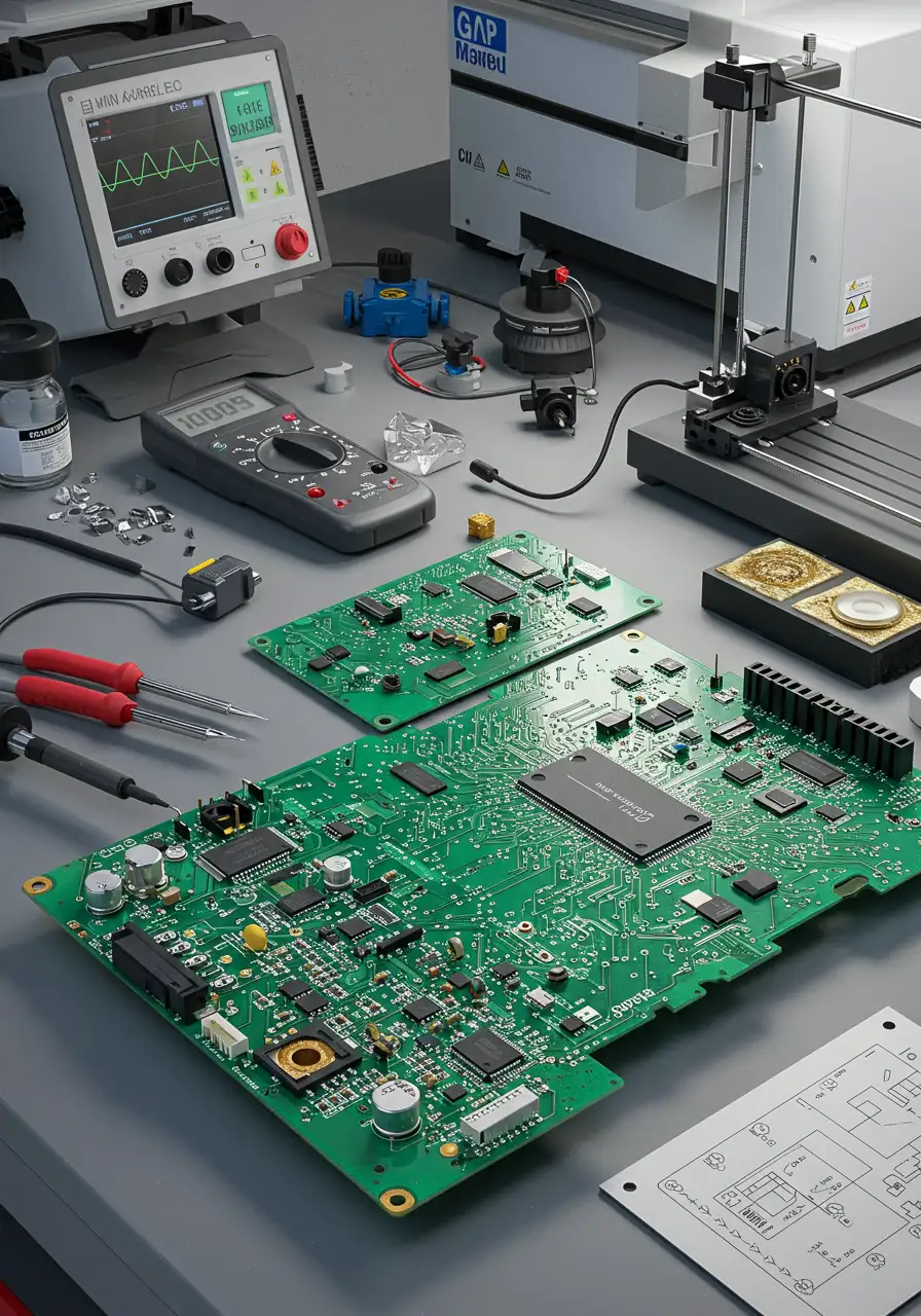
TECHNICAL SPECIFICATIONS
INDUSTRY LEADING FABRICATION TOLERANCES
0.1 mm
MIN TRACE / SPACE
FR4 / Rogers
HIGH FREQ SUBSTRATE
PROJECT GALLERY & RECENT FABRICATIONS
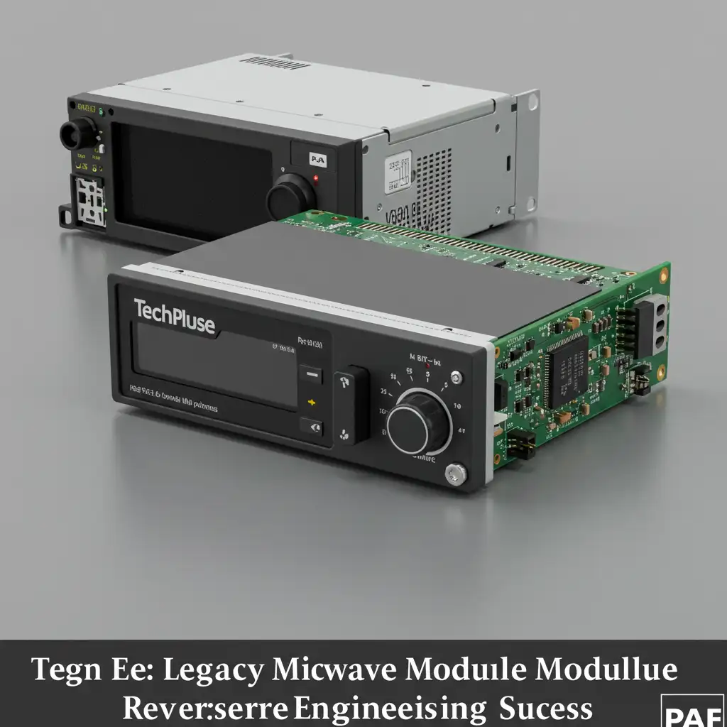
High-Speed Industrial Control Board
Multi-layer impedance matched PCB designed for automated industrial robotics control.
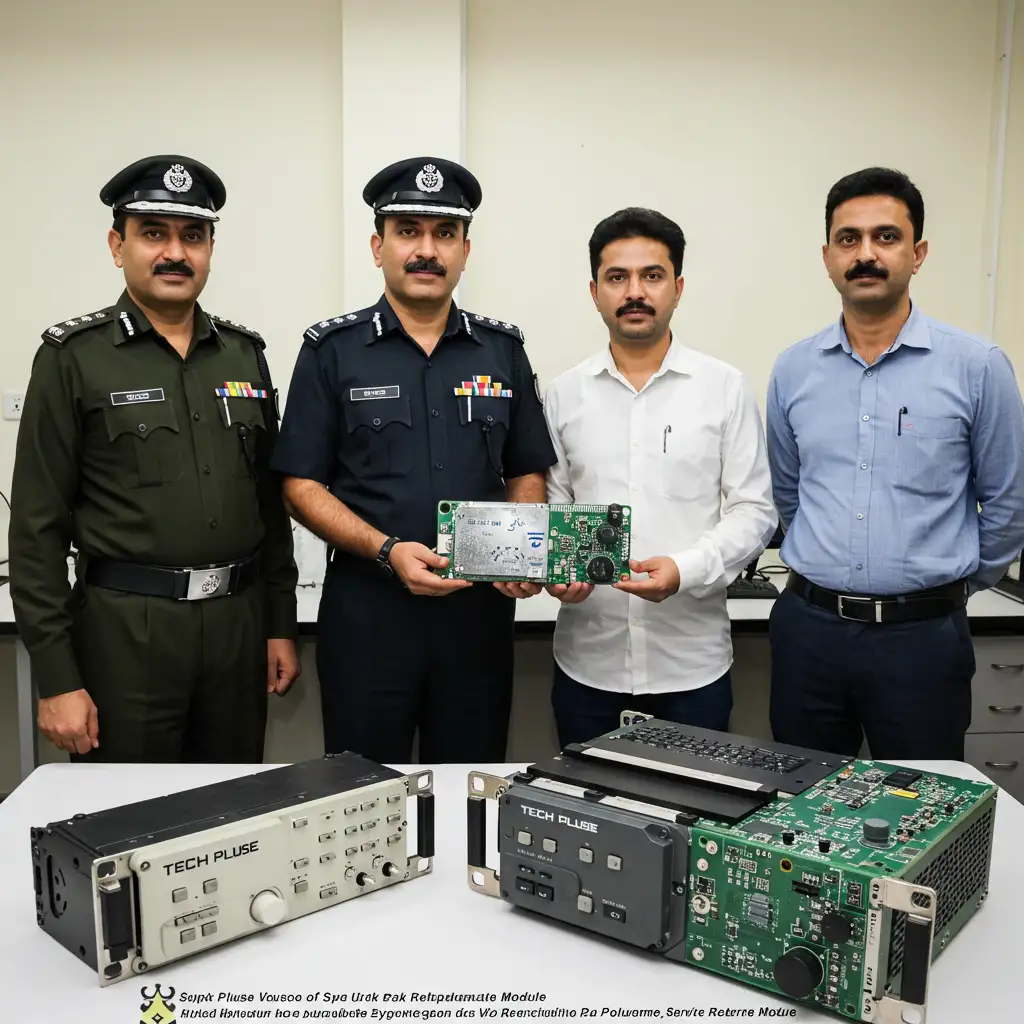
Custom Defense Embedded Module
High-density HDI layout with gold plating for extreme operational temperature environments.